

Hybridisation


Since CMOS pixels contain non-light sensitive elements such as transistors and bus wires they generally perform worse than other optical detectors such as CCDs. Also, since they must be fabricated in Silicon they are limited to a maximum wavelength of about 1um. These limitations can be overcome using the technique of hybridisation. The buses and transistors continue to be fabricated as before in Silicon but the photodiodes are fabricated in a separate layer which is then literally glued down on top of the Silicon. Electrical connections between the two layers are made through tiny "bump bonds" made of the malleable metal Indium. This light sensitive layer does not necessarily need to be made of Silicon. If made from semiconductor alloys such as Mercury Cadmium Tellurium (MCT) then the sensitivity can be extended up to 15um. Hybridisation is an extremely costly process and even relatively small 4Mpix sensors can cost hundreds of thousands of dollars. For many scientific applications it is, however, the only solution.
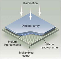
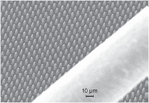
Indium bumps

hair
Credit: Jim Beletic, Teledyne